Simple Push-Pull MOSFET Driver: Protect Your Microcontroller
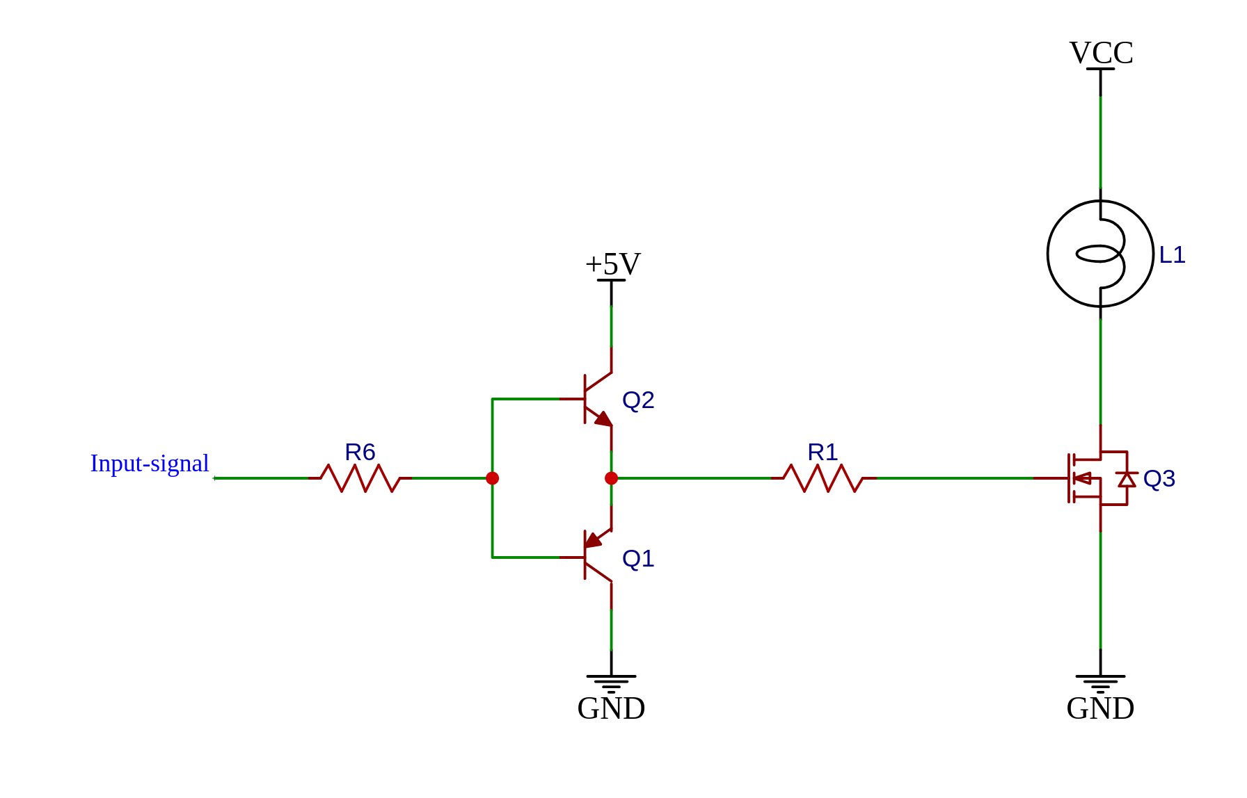
Standard microcontroller IO pins can't always handle the peak current needed to charge a MOSFET's gate capacitance quickly. This discrete push-pull driver using BC547 (NPN) and BC557 (PNP) transistors acts as a high-current buffer, protecting your Arduino or ESP32 while allowing for much faster PWM switching speeds.
| Component | Value/Part | Role |
|---|---|---|
| MOSFET | 6035AL | High-current switch |
| Q1 | BC557 (PNP) | Gate discharge (Pull-down) |
| Q2 | BC547 (NPN) | Gate charge (Push-up) |
| R1 | 100 Ohm | Gate ringing protection |
| R6 | 1k Ohm | Logic signal current limit |
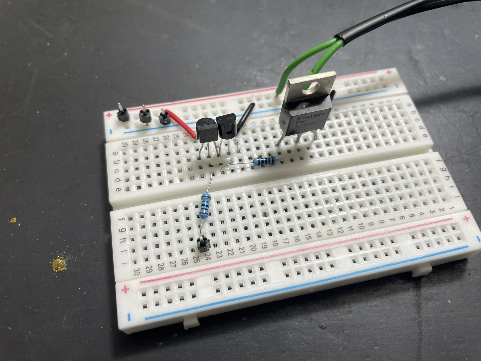
Breadboard
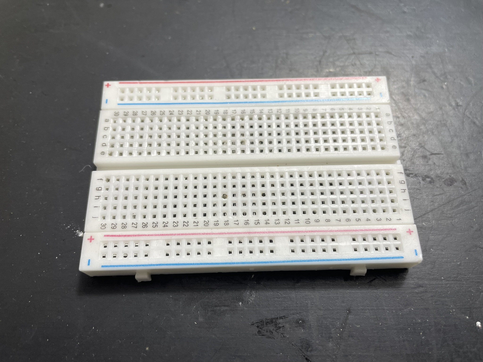
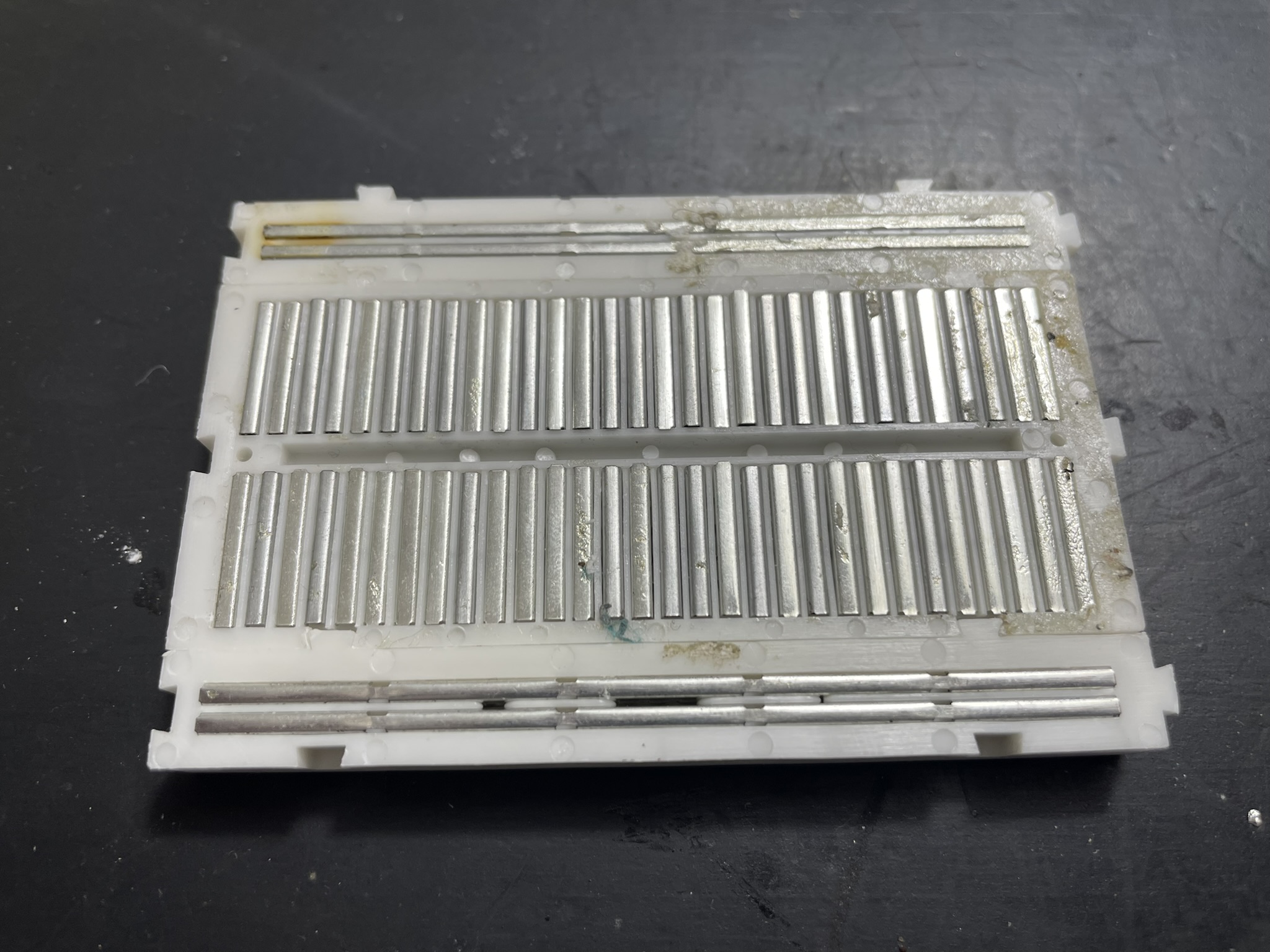
The breadboard I will use for this example, always nice to know what we are working with.
The MOSFET
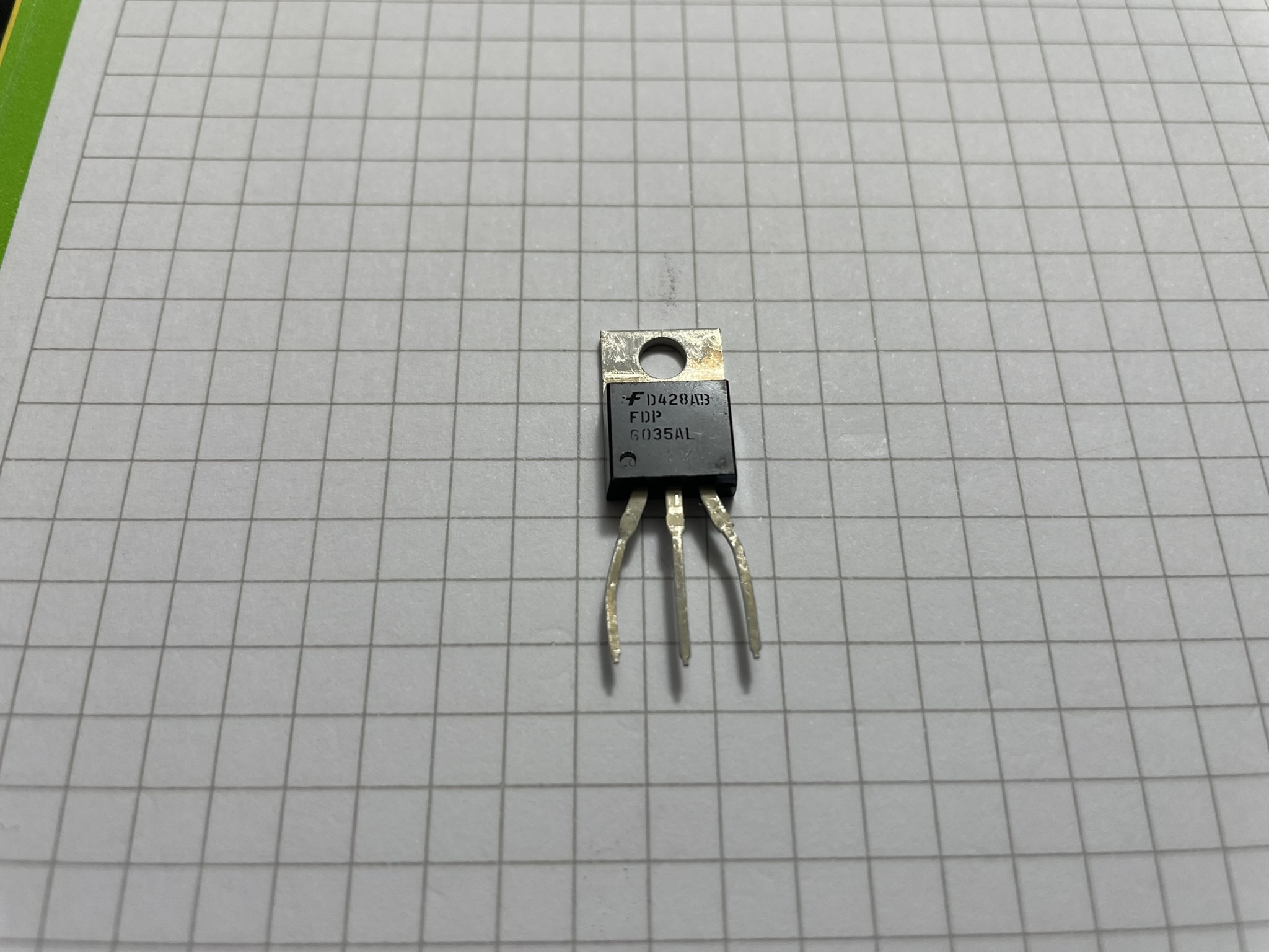
This MOSFET is the 6035AL logic level MOSFET, I got it from AliExpress. Even with 3.3V at its gate it can already switch 30A.
Bicycle light
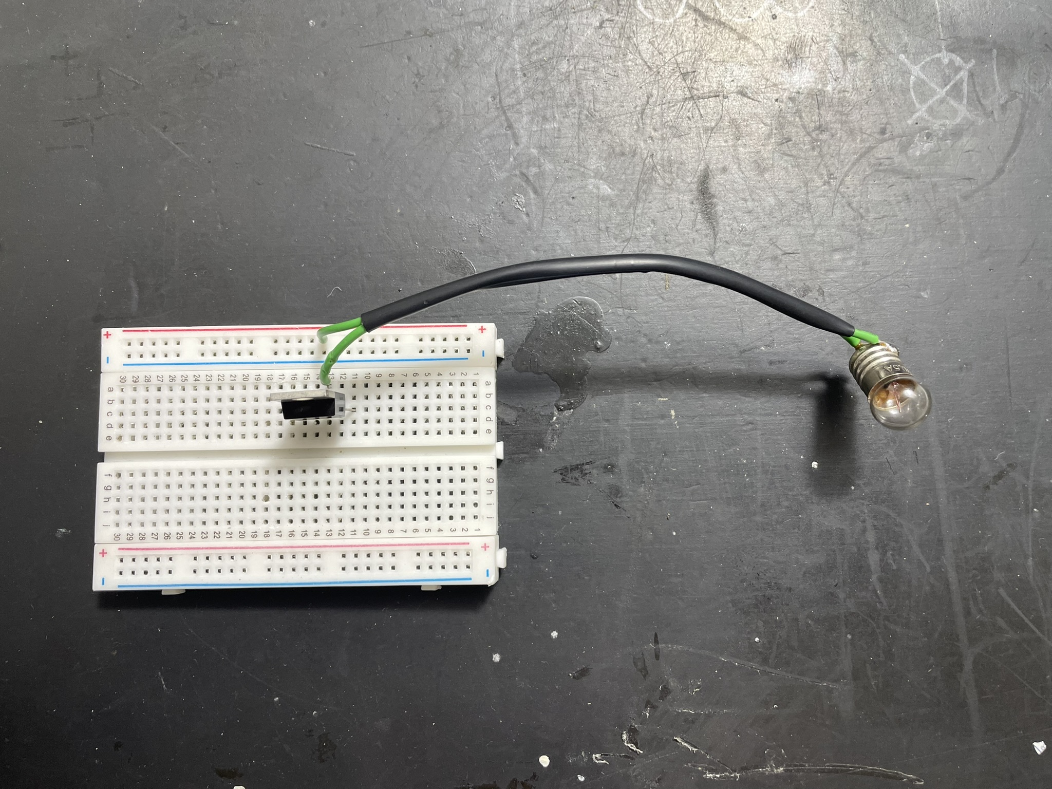
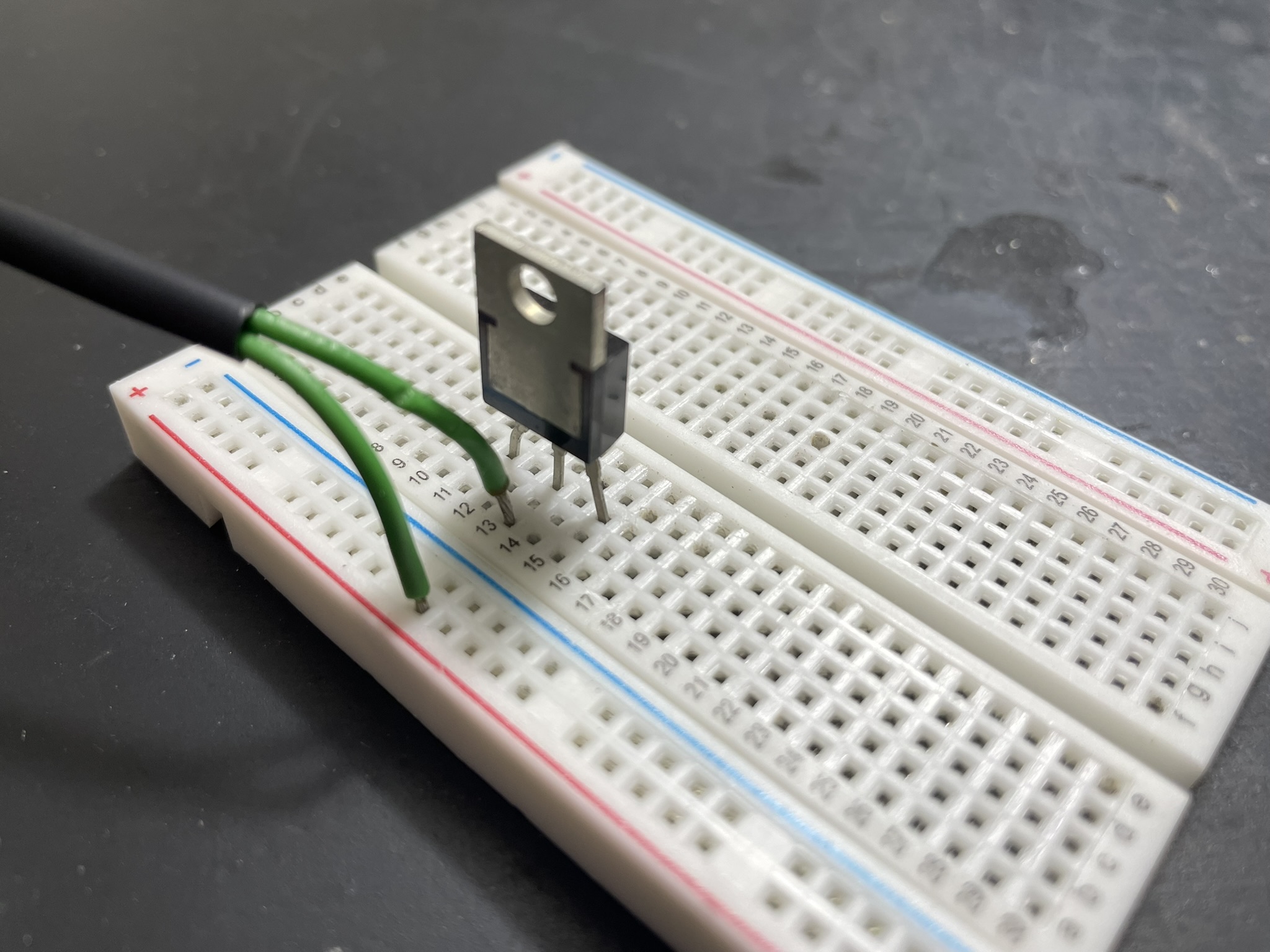
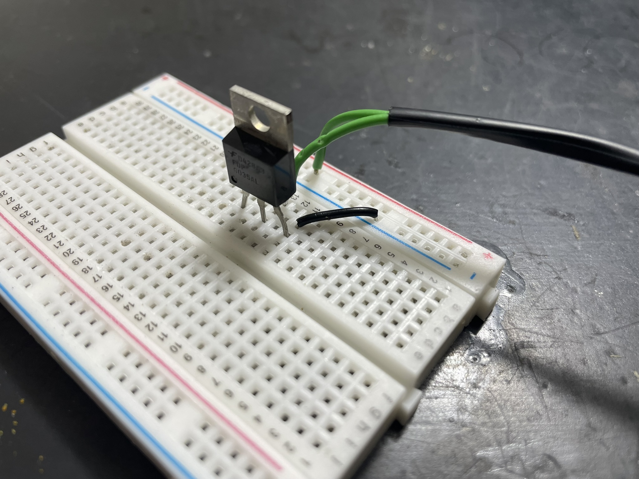
This light bulb does not consume 30A, that would make for a very bright light, and impossible to photograph or film.
These were used on bicycle headlights many years ago before LEDs became cheap enough.
This is a low side switching circuit, so one wire to the bulb goes into the positive power rail, and the other into the drain pin of the MOSFET.
That pin, when the MOSFET is on, connects to the source pin.
From there we connect to ground to complete the circuit.
Bottom transistor Q1
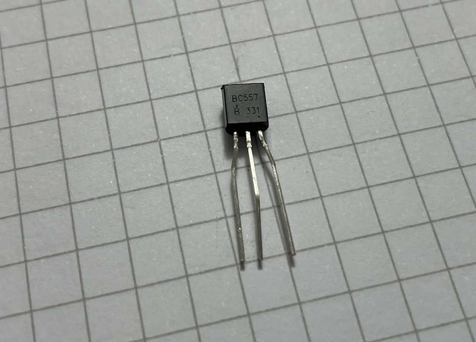
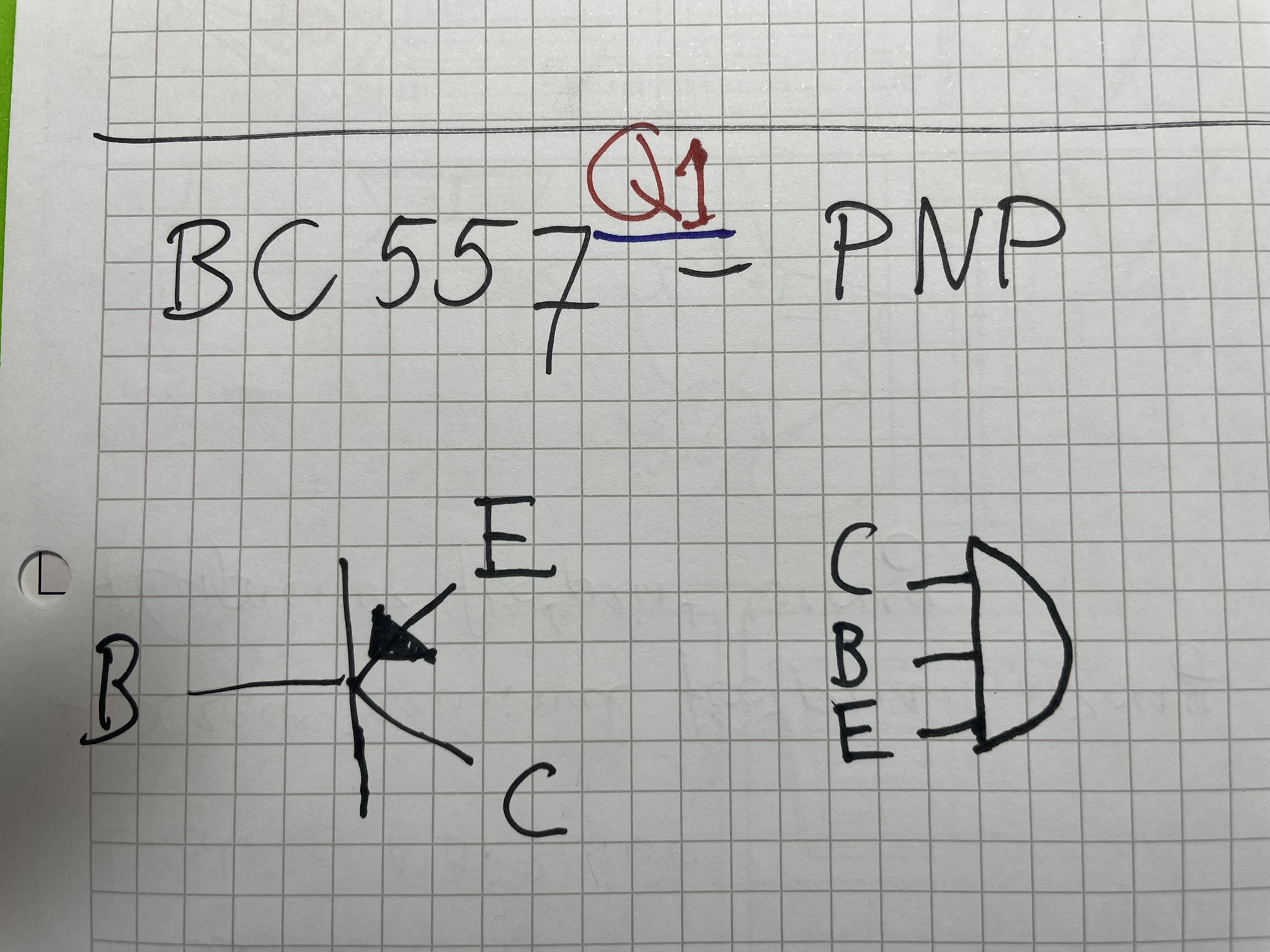
This is a PNP transistor. When the voltage at the base is lower than that on the emitter, It will start conducting. That will make the MOSFET's gate voltage - that is connected to the emitter pins of both transistors - drop to ground.
I always draw the pinout and schematic to a piece of paper because somehow, I easily get the pins mixed up and burn the transistors when testing.
Top transistor Q2
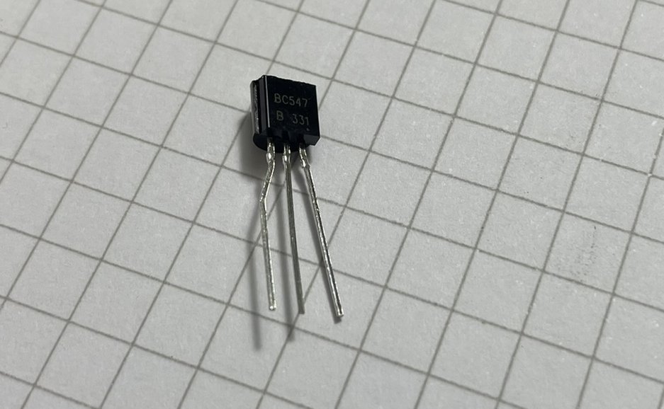
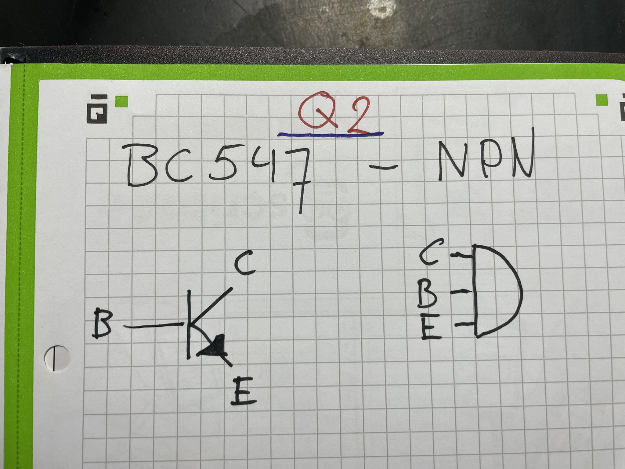
This is a NPN transistor. If we raise the voltage at the base to a higher voltage than is at the emitter, then it will start to conduct. Raising the MOSFET's gate voltage - still connected to the shared emitter pins - to VCC.
Together they make this a voltage follower, where the transistors take a small signal and turn it into a higher current driver.
Transistor pinout
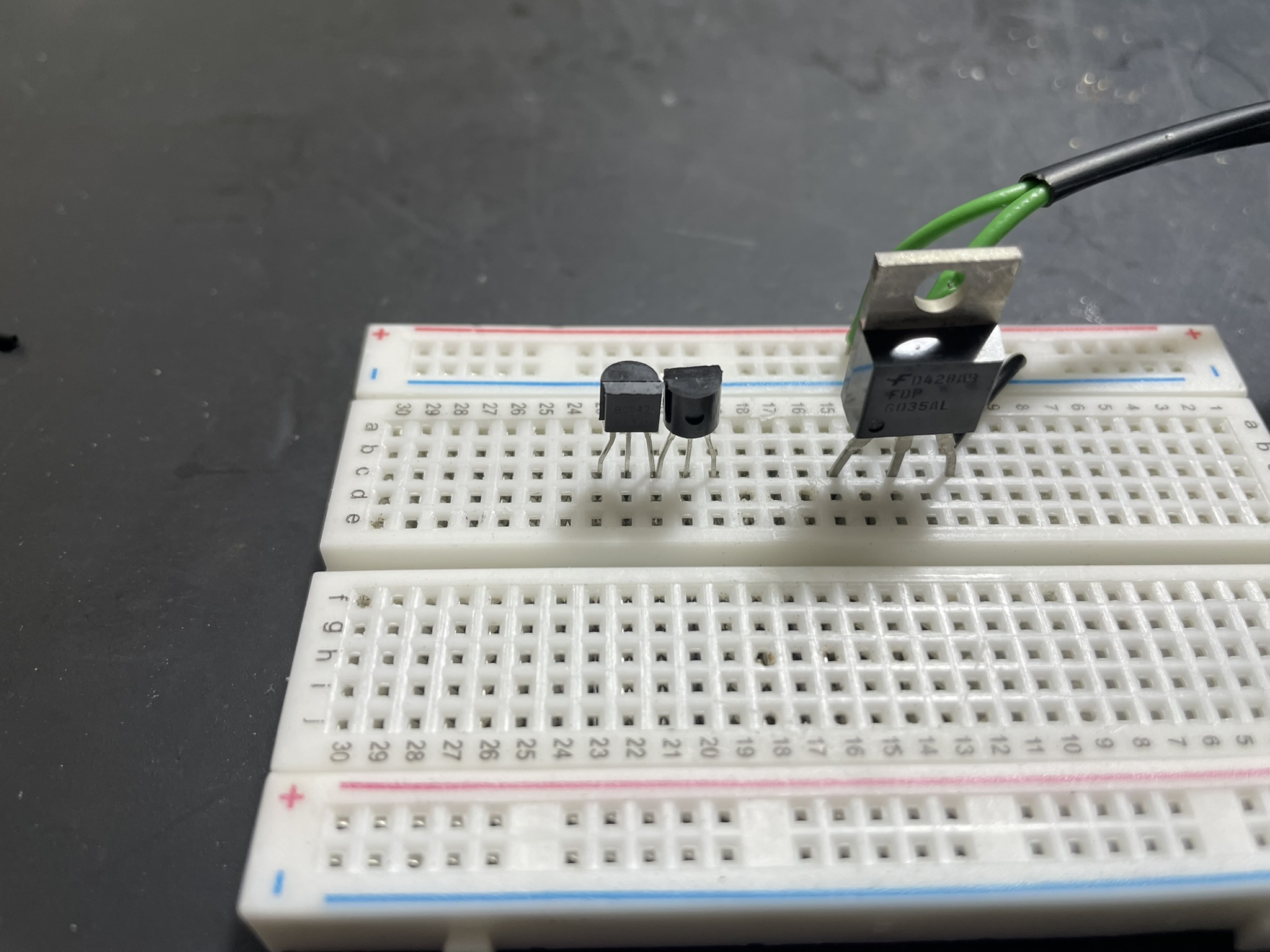
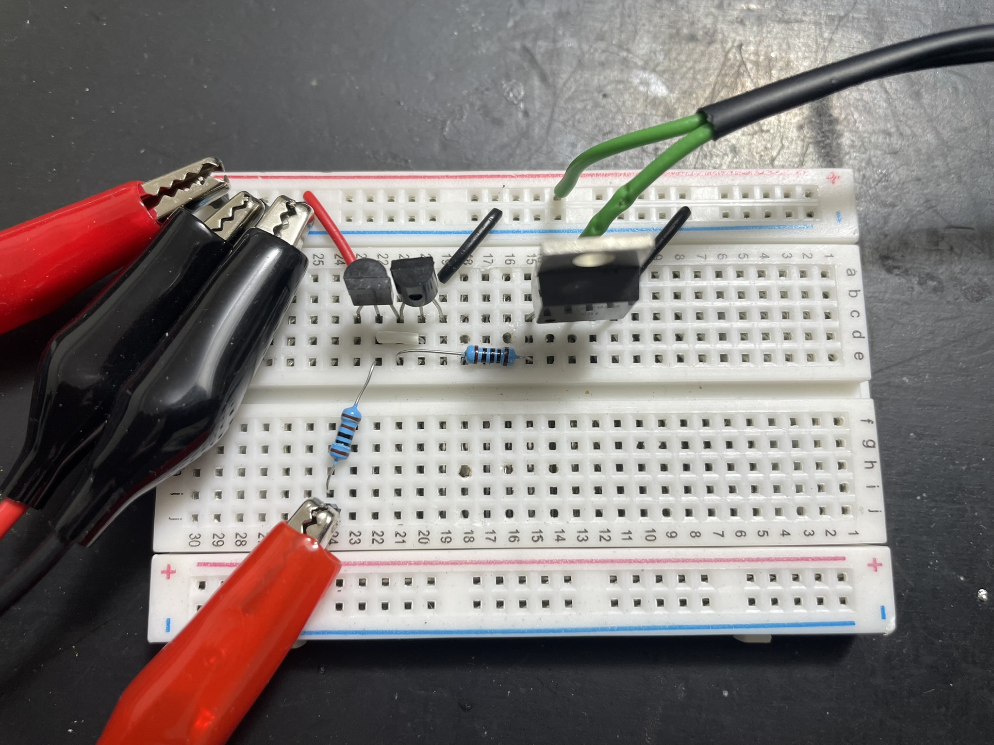
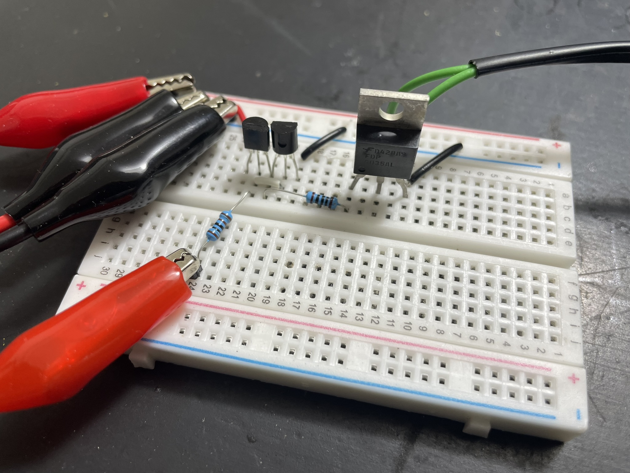
When placed on the breadboard, the NPN and PNP transistors are not oriented in the same direction. And this is why I draw them on paper first, I never get them right the first time.
VCC and ground
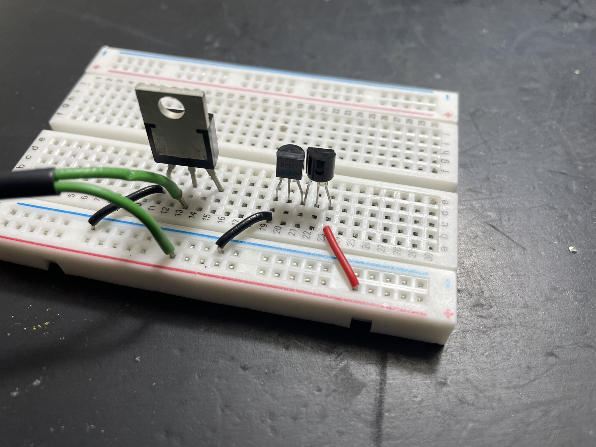
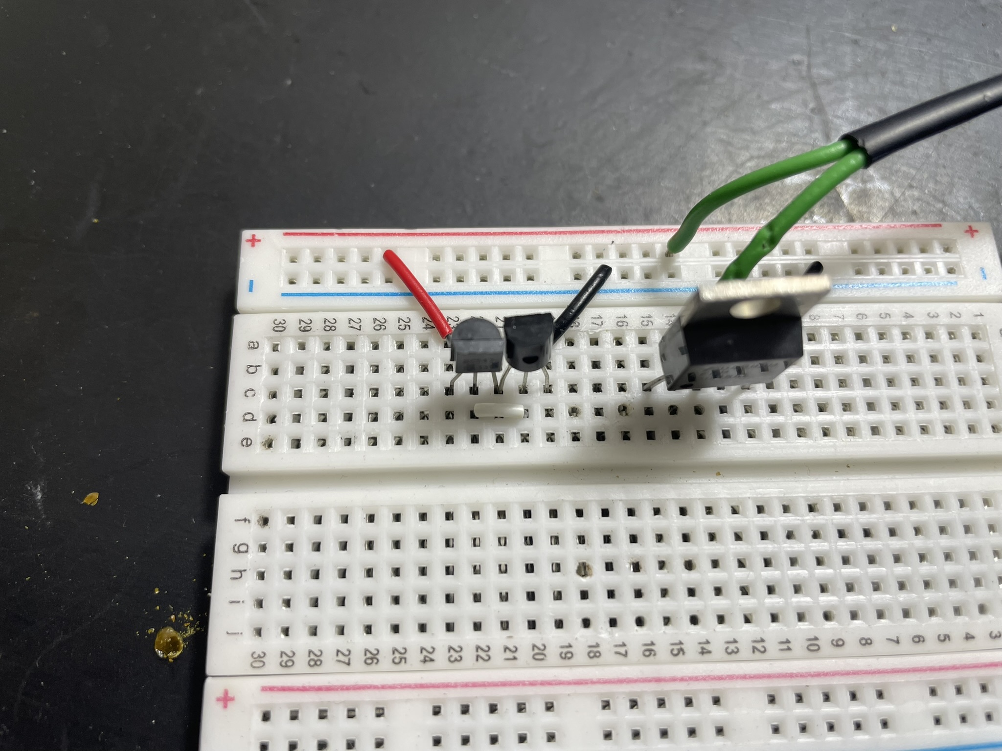
Transistor Q2 needs a connection to VCC, so it can power the gate of the MOSFET.
And transistor Q1 needs a connection to ground, to be able to turn it off again.
Please note that because they are transistors, they will never be conducting at the same time when controlled with the same signal. If these were MOSFETs, that would be a serious issue.
Want to know more about this? Let me know!
Gate resistor R1
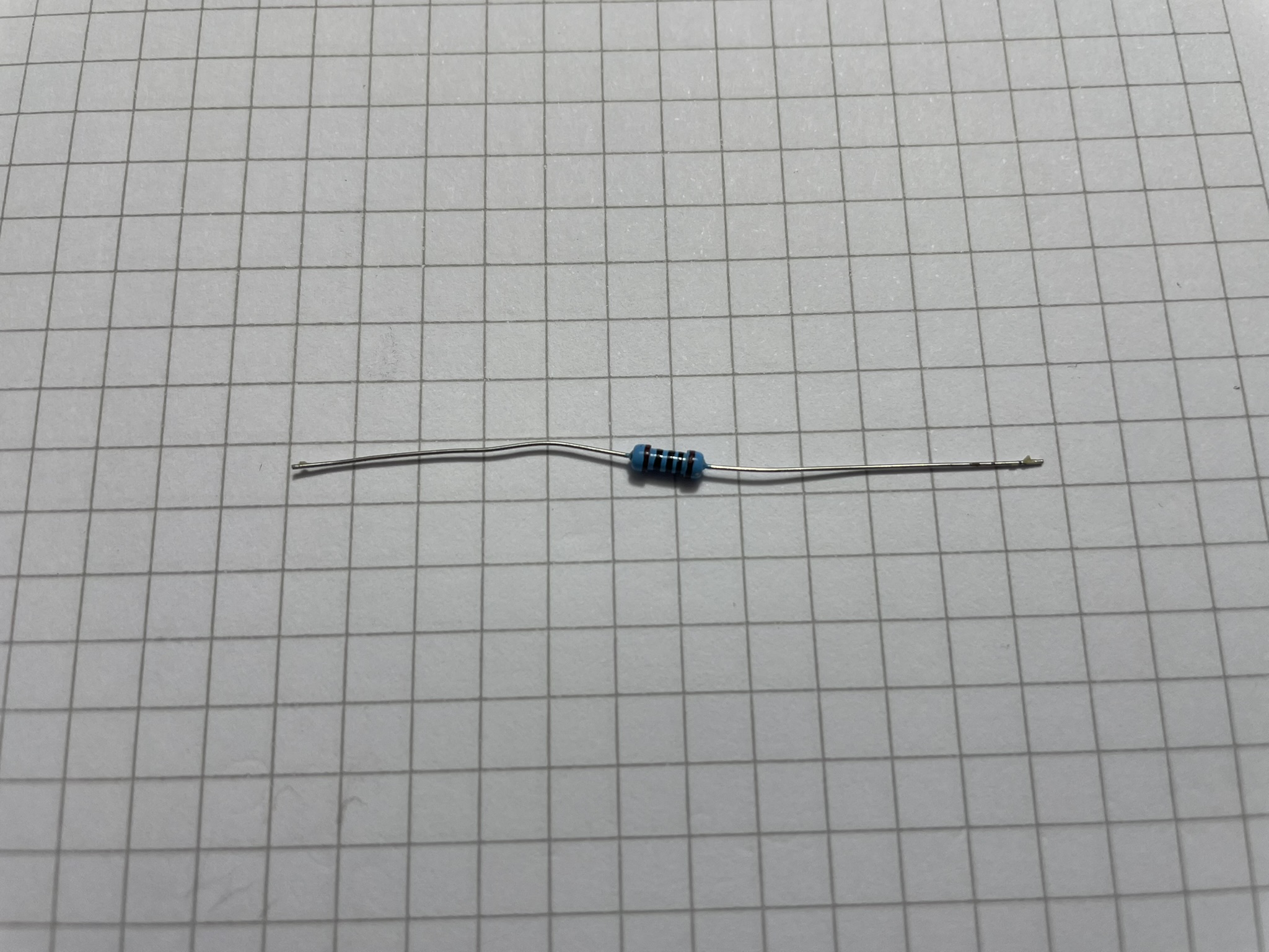
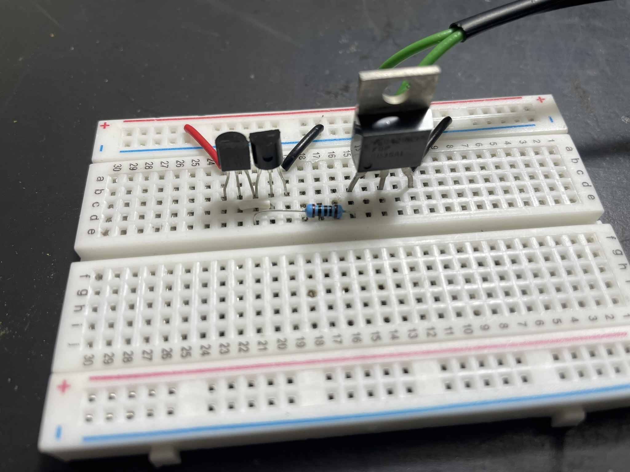
This is a low value resistor (100 ohms) to prevent ringing at the gate of the MOSFET. That becomes an issue when switching the MOSFET at a higher PWM frequency.
And because of the low value it can be very taxing on a microcontrollers IO pin. The peak current draw will be too high during switching. Which is why this circuit exists.
Logic input resistor R6
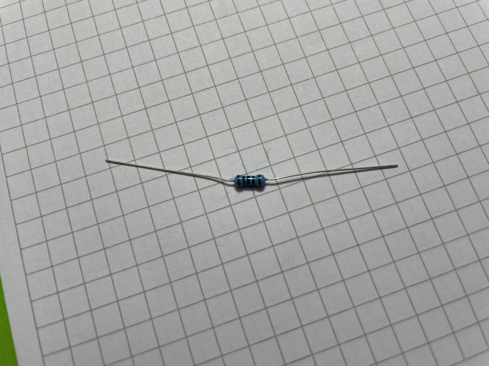
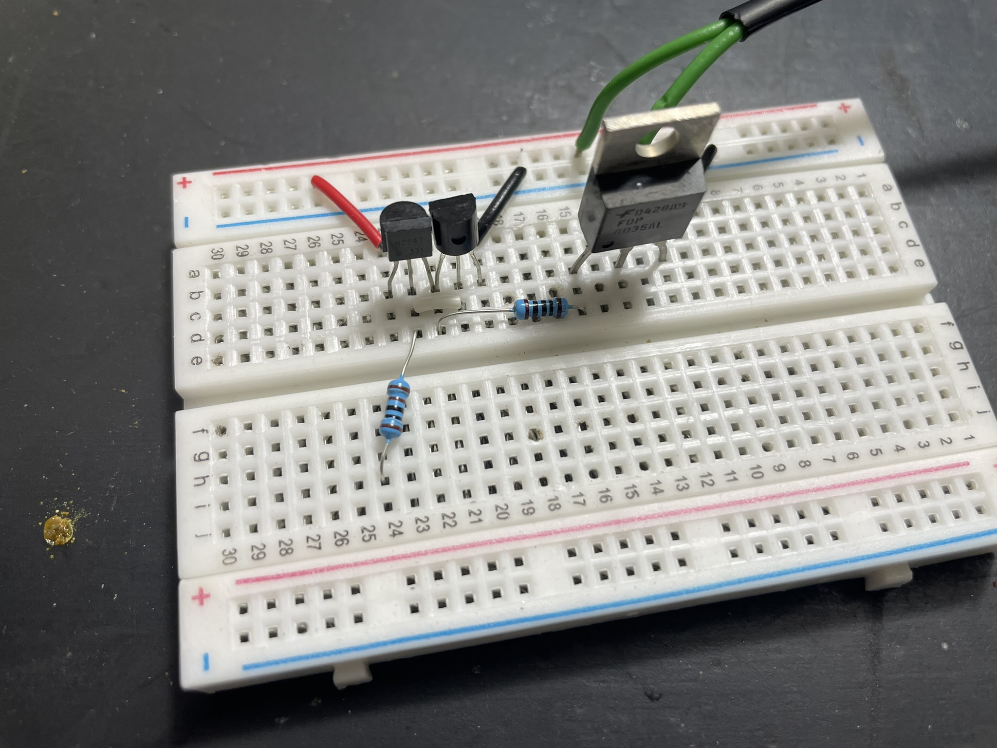
With the transistors in place and doing the heavy (current) lifting. We can now limit the current from the IO input to a safe level. We do this with a 1K ohms resistor.
Adding pins, power and signal